Powering North America's Future, One Chip at a Time
Great Lakes Semiconductor (GLS) is building a new kind of semiconductor company. We are an integrated innovation ecosystem designed to strengthen North America’s capacity to design and develop semiconductor devices, rapidly produce prototype and small-volume wafers, provide advanced packaging and test. We will accelerate the transition from innovation to commercial production of the essential-node semiconductor technologies that power AI, advanced manufacturing, healthcare, transportation, defense, communications, and critical infrastructure.
At the center of this ecosystem are GLS’s ChipForge™ facilities, which integrate Fab-as-a-Service (FaaS™), flexible prototype and low-volume manufacturing, advanced Fab Integrated Packaging and Test (FINPAT™), applied research, engineering services, and workforce development. Through strategic collaborations with industry, government, universities, and global technology leaders, including S2AI, NEITAS and Daikin of Japan, APES, AltaScient, and other ecosystem partners, GLS is creating a more agile, secure, and responsive semiconductor supply chain capable of rapidly bringing next-generation devices from concept to production while supporting the foundational semiconductor technologies that enable the AI economy.
GLS is not building just another semiconductor company. We are building a semiconductor ecosystem that essential industries need while filling critical supply chain gaps. Our mission is to make semiconductor innovation faster, more accessible, and more resilient by bringing together technology, manufacturing, packaging, talent, and strategic partnerships within a single collaborative platform. While much of the industry focuses on the smallest process nodes, GLS is dedicated to advancing the essential-node semiconductors, sensors, MEMS devices, advanced packaging, and heterogeneous integration technologies that underpin artificial intelligence and countless mission-critical applications. Through this stewardship-driven approach, GLS seeks not only to strengthen North America’s semiconductor capabilities today, but to build an enduring foundation for innovation, economic growth, and technological leadership for decades to come.
In summary:
- Why Does GLS Exist? To strengthen North America’s essential-node semiconductor capacity.
- How Does GLS Do It? As an integrated ecosystem built around FaaS™, FINPAT™, ChipForge™, partnerships, and workforce development.
- What Does GLS Deliver? Faster innovation, resilient supply chains, commercialization, and long-term stewardship.
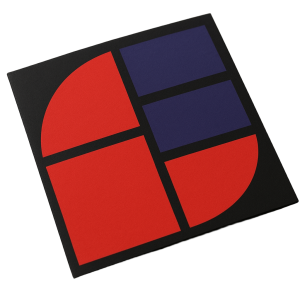
What Great Lakes Semiconductor Stands For.
Our logo is more than a corporate mark, it reflects the philosophy upon which Great Lakes Semiconductor is being built.
Five Core Elements of the Semiconductor Manufacturing Process:
- The five interconnected elements symbolize the integration of technologies, people, and partnerships required to create a resilient semiconductor ecosystem. They also represent our belief that enduring organizations are built by balancing innovation with stewardship, precision with adaptability, and economic growth with long-term responsibility.
- The number five carries special significance. It reflects the five human senses that connect us to the world and underscores GLS’s early focus on sensor technologies. Across many cultures, the number five also represents balance and harmony. In Japanese tradition, the five elements are Earth, Water, Fire, Wind, and the Void. In Chinese and Korean traditions, they are Earth, Fire, Water, Metal, and Wood. While these traditions differ, each recognizes that lasting strength comes from the interaction of complementary elements rather than from any single one alone.
- That same philosophy guides Great Lakes Semiconductor. Success in the semiconductor industry is not achieved through manufacturing alone, but through the integration of research, design, fabrication, advanced packaging, testing, artificial intelligence, workforce development, supply-chain resilience, and trusted partnerships.
The Five Core Business Principles of Great Lakes Semiconductor:
- Innovation & Integration: The smooth, rounded edges represent the seamless integration of design, prototyping, fabrication, advanced packaging, testing, AI-enabled manufacturing, and supply-chain intelligence into a unified semiconductor ecosystem that accelerates innovation from concept to production.
- Collaboration & Stewardship: Great Lakes Semiconductor is founded on the principle that lasting success is achieved through responsible stewardship and meaningful collaboration among industry, government, academia, investors, suppliers, and customers. Together, we strengthen North America’s semiconductor capabilities while creating enduring value for future generations.
- Precision & Resilience: Inspired by the Great Lakes themselves, the flowing contours symbolize precision engineering, reliability, adaptability, and operational resilience, qualities essential to advanced semiconductor manufacturing and secure supply chains.
- Heritage & Vision: The logo reflects the enduring industrial strength and technological heritage of North America while expressing a forward-looking vision for the next generation of semiconductor innovation, workforce development, and economic leadership.
- Scalability & Sustainable Growth: The flowing design represents a flexible ecosystem capable of growing from design to prototype development and small-batch manufacturing, while expanding through the GLS ChipForge™, FINPAT™, and FaaS™ platforms into a globally connected network of semiconductor innovation.
Finally, the five elements symbolize the five great personal influences on Dr. Thurston in conceptualizing and making this disruptive business a reality: E. Lawton Thurston, Jr., Yvonne Thurston, Jerry R. Junkins, Akira Ishikawa, and Dr. Chung-mou (Morris) Chang.